- 您现在的位置:买卖IC网 > Sheet目录1992 > CYW305OXC (Silicon Laboratories Inc)IC CLOCK W305 SOLANO 56SSOP
W305B
........................ Document #: 38-07262 Rev. *B Page 2 of 20
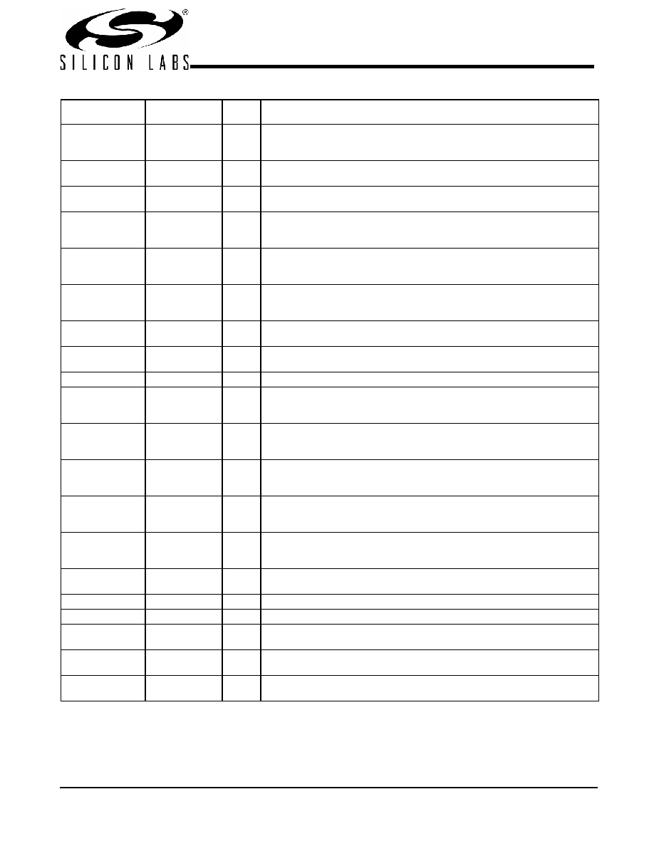
Pin Definitions
Pin Name
Pin No.
Pin
Type
Pin Description
REF2X/FS3
3
I/O
Reference Clock with 2x Drive/Frequency Select 3. 3.3V 14.318-MHz clock
output. This pin also serves as the select strap to determines device operating
frequency as described in Table 5.
X1
4
I
Crystal Input. This pin has dual functions. It can be used as an external
14.318-MHz crystal connection or as an external reference frequency input.
X2
5
O
Crystal Output. An input connection for an external 14.318-MHz crystal
connection. If using an external reference, this pin must be left unconnected.
PCI0/FS0
11
I/O
PCI Clock 0/Frequency Selection 0. 3.3V 33-MHz PCI clock outputs. This pin
also serves as the select strap to determine device operating frequency as
described in Table 5.
PCI1/FS1
12
I/O
PCI Clock 1/Frequency Selection 1. 3.3V 33-MHz PCI clock outputs. This pin
also serves as the select strap to determine device operating frequency as
described in Table 5.
PCI2/FS2
13
I/O
PCI Clock 2/Frequency Selection 2. 3.3V 33-MHz PCI clock outputs. This pin
also serves as the select strap to determine device operating frequency as
described in Table 5.
PCI3:7
15, 16, 18, 19, 20
O
PCI Clock 3 through 7. 3.3V 33-MHz PCI clock outputs. PCI0:7 can be individ-
ually turned off via SMBus interface.
3V66_0:2
7, 8, 9
O
66-MHz Clock Output. 3.3V output clocks. The operating frequency is
controlled by FS0:4 (see Table 5).
48MHz
22
O
48MHz. 3.3V 48-MHz non-spread spectrum output.
48MHz/FS4
23
I/O
48-MHz Output/Frequency Selection 4. 3.3V 48-MHz non-spread spectrum
output. This pin also serves as the select strap to determine device operating
frequency as described in Table 5.
24_48MHz/SEL24
_48MHz#
24
I/O
24- or 48-MHz Output/Select 24 or 48MHz. 3.3V 24 or 48-MHz non-spread
spectrum output. This pin also serves as the select strap to determine the output
frequency for 24_48MHz output.
RST#
30
O
(open-d
rain)
Reset#. Open-drain RESET# output.
CPU0:1
52, 51
O
CPU Clock Outputs. Clock outputs for the host bus interface. Output
frequencies depending on the configuration of FS0:4. Voltage swing is set by
VDDQ2.
SDRAM0:12,
49, 48, 47, 44,
43, 42, 41, 38,
37, 36, 35, 32, 31
O
SDRAM Clock Outputs. 3.3V outputs for SDRAM and chipset. The operating
frequency is controlled by FS0:4 (see Table 5).
APIC
55
O
Synchronous APIC Clock Outputs. Clock outputs running synchronous with
the PCI clock outputs. Voltage swing set by VDDQ2.
SDATA
26
I/O
Data pin for SMBus circuitry.
SCLK
29
I
Clock pin for SMBus circuitry.
VDDQ3
2, 6, 17, 25, 28,
34, 40, 46
P
3.3V Power Connection. Power supply for SDRAM output buffers, PCI output
buffers, reference output buffers and 48-MHz output buffers. Connect to 3.3V.
VDDQ2
53, 56
P
2.5V Power Connection. Power supply for APIC and CPU output buffers.
Connect to 2.5V.
GND
1, 10, 14, 21, 27,
33, 39, 45, 50, 54
G
Ground Connections. Connect all ground pins to the common system ground
plane.
发布紧急采购,3分钟左右您将得到回复。
相关PDF资料
DAC5674IPHPG4
IC DAC 14BIT 400MSPS 48-HTQFP
DAC7621EBG4
IC SNGL 12BIT PARALLEL D/A 20SSO
DAC7801KPG4
IC DUAL 12BIT CMOS DAC 24-DIP
DAC8043AESZ
IC DAC 12BIT MULT SRL INP 8SOIC
DAC8043GP
IC DAC 12BIT MULTIPLY CMOS 8-DIP
DAC8221GP
IC DAC 12BIT DUAL W/BUFF 24-DIP
DAC8222GPZ
IC DAC 12BIT DUAL W/BUFF 24DIP
DAC8229FSZ-REEL
IC DAC 8BIT DUAL V-OUT 20SOIC
相关代理商/技术参数
CYW305OXCT
功能描述:时钟发生器及支持产品 Legacy-Sys Clk Intel RSolano Chip W305B RoHS:否 制造商:Silicon Labs 类型:Clock Generators 最大输入频率:14.318 MHz 最大输出频率:166 MHz 输出端数量:16 占空比 - 最大:55 % 工作电源电压:3.3 V 工作电源电流:1 mA 最大工作温度:+ 85 C 安装风格:SMD/SMT 封装 / 箱体:QFN-56
CYW311OXC
功能描述:时钟发生器及支持产品 Sys Clk VIATM Pro266 DDR Chipset W311 DS RoHS:否 制造商:Silicon Labs 类型:Clock Generators 最大输入频率:14.318 MHz 最大输出频率:166 MHz 输出端数量:16 占空比 - 最大:55 % 工作电源电压:3.3 V 工作电源电流:1 mA 最大工作温度:+ 85 C 安装风格:SMD/SMT 封装 / 箱体:QFN-56
CYW311OXCT
功能描述:时钟发生器及支持产品 Sys Clk VIATM Pro266 DDR Chipset W311 DS RoHS:否 制造商:Silicon Labs 类型:Clock Generators 最大输入频率:14.318 MHz 最大输出频率:166 MHz 输出端数量:16 占空比 - 最大:55 % 工作电源电压:3.3 V 工作电源电流:1 mA 最大工作温度:+ 85 C 安装风格:SMD/SMT 封装 / 箱体:QFN-56
CYW312OXC
制造商:SPECTRALINEAR 制造商全称:SPECTRALINEAR 功能描述:FTG for VIA⑩ K7 Series Chipset with Programmable Output Frequency
CYW312OXCT
制造商:CYPRESS 制造商全称:Cypress Semiconductor 功能描述:FTG for VIA⑩ K7 Series Chipset with Programmable Output Frequency
CYW320OXC-3
功能描述:时钟合成器/抖动清除器 Legacy, W320-03 datasheet RoHS:否 制造商:Skyworks Solutions, Inc. 输出端数量: 输出电平: 最大输出频率: 输入电平: 最大输入频率:6.1 GHz 电源电压-最大:3.3 V 电源电压-最小:2.7 V 封装 / 箱体:TSSOP-28 封装:Reel
CYW320OXC-3T
功能描述:时钟合成器/抖动清除器 Legacy, W320-03 datasheet RoHS:否 制造商:Skyworks Solutions, Inc. 输出端数量: 输出电平: 最大输出频率: 输入电平: 最大输入频率:6.1 GHz 电源电压-最大:3.3 V 电源电压-最小:2.7 V 封装 / 箱体:TSSOP-28 封装:Reel
CYW320OXC-4
功能描述:时钟合成器/抖动清除器 Legacy, W320-04 datasheet RoHS:否 制造商:Skyworks Solutions, Inc. 输出端数量: 输出电平: 最大输出频率: 输入电平: 最大输入频率:6.1 GHz 电源电压-最大:3.3 V 电源电压-最小:2.7 V 封装 / 箱体:TSSOP-28 封装:Reel